


Calit2 Semiconductors Winter Training Program
An intensive, hands-on program connecting semiconductor fundamentals to real systems; from devices and
manufacturing to sensing, computing, communication, and application-driven design.
UC Irvine • Calit2 • INRF
Semiconductors & Systems
Program Overview
This winter training program introduces the semiconductor ecosystem and connects it to modern
semiconductor-enabled systems—including IoT and edge AI applications. Participants will explore
how silicon-level constraints shape system design tradeoffs in performance, energy, cost,
reliability, and security.
What you’ll learn
- Semiconductor landscape: supply chain, fabs, packaging, and ecosystem trends
- Materials & equipment: emerging processes and tools (with cleanroom exposure)
- Modern SoCs: CPU + memory + peripherals + radios + security + (sometimes) AI accelerators
- AI semiconductors: specialization for edge/cloud and the efficiency story
- Design tradeoffs: latency vs energy, performance vs area, flexibility vs specialization
Program format
- Interactive lectures and discussions
- Hands-on exposure via INRF cleanroom tours (as scheduled)
- Calit2 lab tours and applied case studies
- Industry excursions
Quick Facts
- DatesJan 13–Jan 30, 2026
- Primary locationsISEB • Calit2 • INRF (Cleanroom)
- FocusSemiconductors → Systems (IoT, Edge AI, Infrastructure)
- ActivitiesLectures • Tours • Cleanroom • Company Excursions
Bring a laptop for note-taking and follow-along materials (when available).
Wear closed-toe shoes for tours.
Industry Excursions
The two excursion days connect the “classroom” view of semiconductors to how chips are designed,
packaged, qualified, and deployed in real products. Each visit is framed around the same workshop
themes—performance/energy tradeoffs, reliability and yield, packaging constraints, and system-level
implications—so participants can relate what they see on the factory/engineering side back to the
device and process content covered earlier.
Day 1 — Navitas Semiconductor
-
What they do: Power semiconductor technologies and power ICs used in fast charging,
power conversion, and high-efficiency systems. -
Why it matters for the workshop: Links device and packaging choices to end-to-end
energy efficiency, thermal constraints, and form-factor limits in real products (e.g., chargers,
adapters, power modules). -
What to look for: How reliability/qualification, thermal design, and packaging
decisions influence system performance and cost.
Day 2 — Tower Semiconductor
-
What they do: Specialty foundry manufacturing (e.g., analog/RF, power management,
sensors) enabling many mixed-signal and sensor-driven systems. -
Why it matters for the workshop: Connects process steps (lithography/etch/deposition/metrology)
to real manufacturing constraints—yield, variability, and how “process reality” shapes what systems can do. -
What to look for: How metrology, process control, and yield considerations drive design rules
and system-level tradeoffs.
workshop concepts (device/process limits → packaging → system architecture → application constraints).
Schedule (01/13–01/30, 2026)
| Date | Time | Instructor / Host | Session / Activity | Location |
|---|---|---|---|---|
| Week 1 (01/13–01/16) | ||||
| 01/13 | 10:00–12:00 | Dr. G. P. Li | Orientation about UCI | ISEB 1200 |
| 01/13 | 14:00–18:00 | Dr. G. P. Li | Campus Tour | ISEB 1200 |
| 01/14 | 10:00–12:00 | Dr. Peter Burke | Semiconductor Industry | ISEB 1200 |
| 01/14 | 14:00–18:00 | Dr. Peter Burke | History of Semiconductor & Development Trends | ISEB 1200 |
| 01/15 | 10:00–12:00 | Dr. Peter Burke | New Technology of Semiconductor Material | ISEB 1200 |
| 01/15 | 14:00–16:00 | Dr. Camilo Velez Cuervo | New Technology of Semiconductor Equipment | ISEB 1200 |
| 01/15 | 16:00–18:00 | Dr. G. P. Li | AI Semiconductor | ISEB 1200 |
| 01/16 | 10:00–12:00 | Dr. G. P. Li | AI Semiconductor | Calit2 |
| 01/16 | 14:00–16:00 | Dr. Boris Vaisband | New Technology of Semiconductor Packaging | Calit2 |
| 01/16 | 16:00–18:00 | Dr. Boris Vaisband | Patent of Semiconductor | Calit2 |
| Week 2 (01/19–01/23) | ||||
| 01/19 | 10:00–12:00 | Dr. Arnold Wang | Calit2 Research Theme: Energy Systems (MLK Day) | Calit2 / Energy |
| 01/19 | 14:00–16:00 | Dr. Lily Wu | Calit2 Research Theme: Microfluidics & BioMEMS (MLK Day) | Calit2 / Microfluidics |
| 01/19 | 16:00–18:00 | Dr. Sergio Gago | Calit2 Research Theme: Semiconductors to Systems (MLK Day) | Calit2 / ETAD |
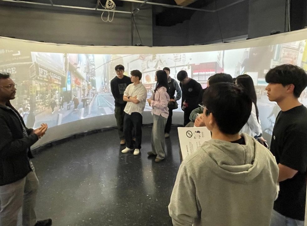
| 01/20 | 10:00–12:00 | Dr. Athina Markopoulou | Welcome to Calit2: Mission, Labs, and Collaboration Model | Calit2 |
| 01/20 | 14:00–18:00 | Dr. G. P. Li | Calit2 Tour (IMRI, Visualization, CalPlug, Labs) | Calit2 (various labs) |
| 01/21 | 10:00–12:00 | Dr. Glenn Healey | Calit2 Research Theme: Environment & Sensing | Calit2 / Environment |
| 01/21 | 14:00–16:00 | Dr. Kylie Peppler | Calit2 Research Theme: Connected Learning | Calit2 / Connected Learning |
| 01/21 | 16:00–18:00 | Dr. G. P. Li | Calit2 Research Theme: Smart Manufacturing | Calit2 / Smart Manufacturing |
| 01/22 | 10:00–12:00 | Dr. Camilo Velez Cuervo | Semiconductor Manufacturing Process I | Litho / Calit2 |
| 01/22 | 14:00–18:00 | Richard Chang | Cleanroom Tour: Lithography process walkthrough | Litho / INRF |
| 01/23 | 10:00–12:00 | Dr. Camilo Velez Cuervo | Semiconductor Manufacturing Process II | Etching / Calit2 |
| 01/23 | 14:00–18:00 | Dr. Mo Kebaili | Cleanroom Tour: Etching process walkthrough | Etching / INRF |
| Week 3 (01/26–01/30) | ||||
| 01/26 | 10:00–12:00 | Dr. Camilo Velez Cuervo | Semiconductor Manufacturing Process III | Deposition / Calit2 |
| 01/26 | 14:00–18:00 | Dr. Chuangyuan Lee | Cleanroom Tour: Deposition process walkthrough | Deposition / INRF |
| 01/27 | 10:00–12:00 | Dr. SungWoo Nam | Semiconductor Manufacturing Process IV | Metrology |
| 01/27 | 14:00–18:00 | Dr. Chuangyuan Lee | Cleanroom Tour: Metrology process walkthrough | Metrology / INRF |
| 01/28 | 10:00–18:00 | Dr. Scott Martin | Company Excursion Day 1: Navitas Semiconductor | Navitas Semiconductor |
| 01/29 | 10:00–18:00 | Dr. G. P. Li | Company Excursion Day 2: Tower Semiconductor | Tower Semiconductor |
| 01/30 | 10:00–12:00 | Dr. G. P. Li | Graduation Ceremony & Farewell | Calit2 |